• About Us
  • Contact Us
  • Terms & Conditions
  • Privacy Policy
Technology Hive
  • Home
  • Technology
  • Artificial Intelligence (AI)
  • Cyber Security
  • Machine Learning
  • More
    • Deep Learning
    • AI in Healthcare
    • AI Regulations & Policies
    • Business
    • Cloud Computing
    • Ethics & Society
No Result
View All Result
  • Home
  • Technology
  • Artificial Intelligence (AI)
  • Cyber Security
  • Machine Learning
  • More
    • Deep Learning
    • AI in Healthcare
    • AI Regulations & Policies
    • Business
    • Cloud Computing
    • Ethics & Society
No Result
View All Result
Technology Hive
No Result
View All Result
Home Artificial Intelligence (AI)

MIT engineers grow ‘high-rise’ 3D chips

Adam Smith – Tech Writer & Blogger by Adam Smith – Tech Writer & Blogger
March 6, 2025
in Artificial Intelligence (AI)
0
MIT engineers grow ‘high-rise’ 3D chips
0
SHARES
0
VIEWS
Share on FacebookShare on Twitter

The Future of Electronics: Building Up Instead of Out

The Limitations of Current Technology

The electronics industry is approaching a limit to the number of transistors that can be packed onto the surface of a computer chip. To overcome this limitation, chip manufacturers are looking to build up rather than out. This means stacking multiple surfaces of transistors and semiconducting elements, similar to turning a ranch house into a high-rise. Such multilayered chips could handle exponentially more data and carry out many more complex functions than today’s electronics.

The Challenge of Stacking Chips

However, a significant hurdle is the platform on which chips are built. Today, bulky silicon wafers serve as the main scaffold on which high-quality, single-crystalline semiconducting elements are grown. Any stackable chip would have to include thick silicon "flooring" as part of each layer, slowing down any communication between functional semiconducting layers.

MIT Engineers’ Breakthrough

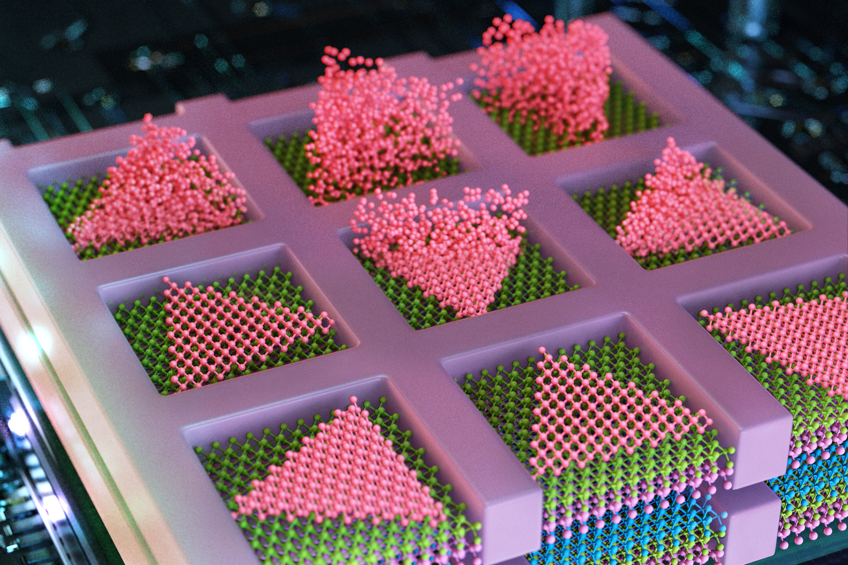
Now, MIT engineers have found a way around this hurdle, with a multilayered chip design that doesn’t require any silicon wafer substrates and works at temperatures low enough to preserve the underlying layer’s circuitry. In a study published in the journal Nature, the team reports using this new method to fabricate a multilayered chip with alternating layers of high-quality semiconducting material grown directly on top of each other.

How It Works

The method enables engineers to build high-performance transistors and memory and logic elements on any random crystalline surface – not just on the bulky crystal scaffold of silicon wafers. Without these thick silicon substrates, multiple semiconducting layers can be in more direct contact, leading to better and faster communication and computation between layers, the researchers say.

The Future of AI and Computing

The researchers envision that the method could be used to build AI hardware, in the form of stacked chips for laptops or wearable devices, that would be as fast and powerful as today’s supercomputers and could store huge amounts of data on par with physical data centers. "This breakthrough opens up enormous potential for the semiconductor industry, allowing chips to be stacked without traditional limitations," says study author Jeehwan Kim, associate professor of mechanical engineering at MIT. "This could lead to orders-of-magnitude improvements in computing power for applications in AI, logic, and memory."

Conclusion

The development of stackable chips has the potential to revolutionize the electronics industry, enabling the creation of faster, more powerful, and more efficient devices. With the help of this new technology, we can build AI hardware that is more powerful and efficient, leading to significant advancements in various fields, from healthcare to finance to education.

Frequently Asked Questions

Q: What is the purpose of the new method?
A: The new method enables the fabrication of multilayered chips without the need for silicon wafer substrates, allowing for faster and more efficient communication between layers.

Q: How does the new method work?
A: The method uses a technique known as "nucleation" to grow single-crystalline 2D materials at low temperatures, allowing for the creation of high-quality semiconducting materials on any random crystalline surface.

Q: What are the potential applications of this technology?
A: The technology has the potential to be used to build AI hardware, such as stacked chips for laptops or wearable devices, that would be as fast and powerful as today’s supercomputers and could store huge amounts of data on par with physical data centers.

Previous Post

Understanding and Calculating the Median

Next Post

What’s happening nationally and globally with telehealth, AI and cybersecurity

Adam Smith – Tech Writer & Blogger

Adam Smith – Tech Writer & Blogger

Adam Smith is a passionate technology writer with a keen interest in emerging trends, gadgets, and software innovations. With over five years of experience in tech journalism, he has contributed insightful articles to leading tech blogs and online publications. His expertise covers a wide range of topics, including artificial intelligence, cybersecurity, mobile technology, and the latest advancements in consumer electronics. Adam excels in breaking down complex technical concepts into engaging and easy-to-understand content for a diverse audience. Beyond writing, he enjoys testing new gadgets, reviewing software, and staying up to date with the ever-evolving tech industry. His goal is to inform and inspire readers with in-depth analysis and practical insights into the digital world.

Related Posts

AI-Powered Next-Gen Services in Regulated Industries
Artificial Intelligence (AI)

AI-Powered Next-Gen Services in Regulated Industries

by Adam Smith – Tech Writer & Blogger
June 13, 2025
NVIDIA Boosts Germany’s AI Manufacturing Lead in Europe
Artificial Intelligence (AI)

NVIDIA Boosts Germany’s AI Manufacturing Lead in Europe

by Adam Smith – Tech Writer & Blogger
June 13, 2025
The AI Agent Problem
Artificial Intelligence (AI)

The AI Agent Problem

by Adam Smith – Tech Writer & Blogger
June 12, 2025
The AI Execution Gap
Artificial Intelligence (AI)

The AI Execution Gap

by Adam Smith – Tech Writer & Blogger
June 12, 2025
Restore a damaged painting in hours with AI-generated mask
Artificial Intelligence (AI)

Restore a damaged painting in hours with AI-generated mask

by Adam Smith – Tech Writer & Blogger
June 11, 2025
Next Post
What’s happening nationally and globally with telehealth, AI and cybersecurity

What's happening nationally and globally with telehealth, AI and cybersecurity

Leave a Reply Cancel reply

Your email address will not be published. Required fields are marked *

Latest Articles

UK Must Act to Secure Its Semiconductor Industry Leadership

UK Must Act to Secure Its Semiconductor Industry Leadership

February 26, 2025
AI Transparency vs ‘Open-Washing’

AI Transparency vs ‘Open-Washing’

February 25, 2025
The AI Blockchain Explained

The AI Blockchain Explained

June 10, 2025

Browse by Category

  • AI in Healthcare
  • AI Regulations & Policies
  • Artificial Intelligence (AI)
  • Business
  • Cloud Computing
  • Cyber Security
  • Deep Learning
  • Ethics & Society
  • Machine Learning
  • Technology
Technology Hive

Welcome to Technology Hive, your go-to source for the latest insights, trends, and innovations in technology and artificial intelligence. We are a dynamic digital magazine dedicated to exploring the ever-evolving landscape of AI, emerging technologies, and their impact on industries and everyday life.

Categories

  • AI in Healthcare
  • AI Regulations & Policies
  • Artificial Intelligence (AI)
  • Business
  • Cloud Computing
  • Cyber Security
  • Deep Learning
  • Ethics & Society
  • Machine Learning
  • Technology

Recent Posts

  • Best Practices for AI in Bid Proposals
  • Artificial Intelligence for Small Businesses
  • Google Generates Fake AI Podcast From Search Results
  • Technologies Shaping a Nursing Career
  • AI-Powered Next-Gen Services in Regulated Industries

Our Newsletter

Subscribe Us To Receive Our Latest News Directly In Your Inbox!

We don’t spam! Read our privacy policy for more info.

Check your inbox or spam folder to confirm your subscription.

© Copyright 2025. All Right Reserved By Technology Hive.

No Result
View All Result
  • Home
  • Technology
  • Artificial Intelligence (AI)
  • Cyber Security
  • Machine Learning
  • AI in Healthcare
  • AI Regulations & Policies
  • Business
  • Cloud Computing
  • Ethics & Society
  • Deep Learning

© Copyright 2025. All Right Reserved By Technology Hive.

Are you sure want to unlock this post?
Unlock left : 0
Are you sure want to cancel subscription?